Implementing a FIR filter on FPGA

FIR (Finite impulse response) filter

Overview

Finite impulse response (FIR) filters are characterized by the fact that they use only delayed versions of the input signal to filter the input to the output.
For a causal discrete-time FIR filter of order N, each value of the output sequence is a weighted sum of the most recent input values:
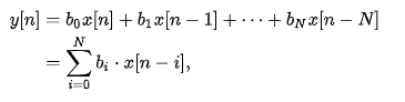
Where:

  • x[n] is the input signal,
  • y[n] is the output signal,
  • N is the filter order
  • bi is the value of the impulse response, also a coefficient of the filter

Filter design

FIR filter designing is finding the coefficients and filter order that meet certain specifications. When a particular frequency response is desired, several different design methods are common:

  • Window design method
  • Frequency sampling method
  • Least MSE (mean square error) method
  • Parks-McClellan method
  • DFT algorithms

There many software such as MATLAB, GNU Octave, Scilab and SciPy (Python).
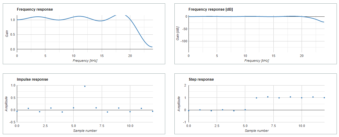
In this topic, I only share how to implement FIR filter on FPGA. So the detail of filter designing, finding coefficients will shared in the later topics.

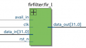
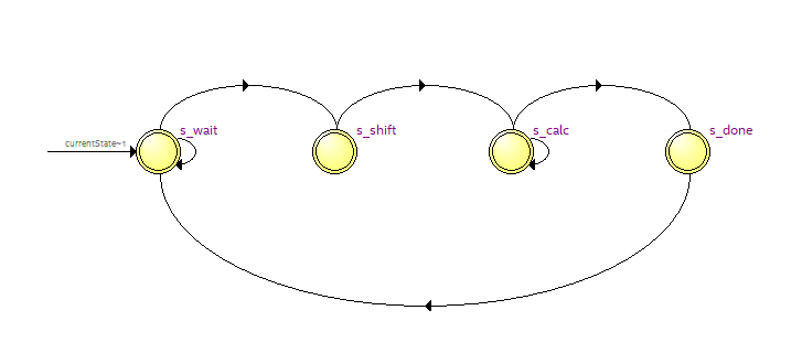
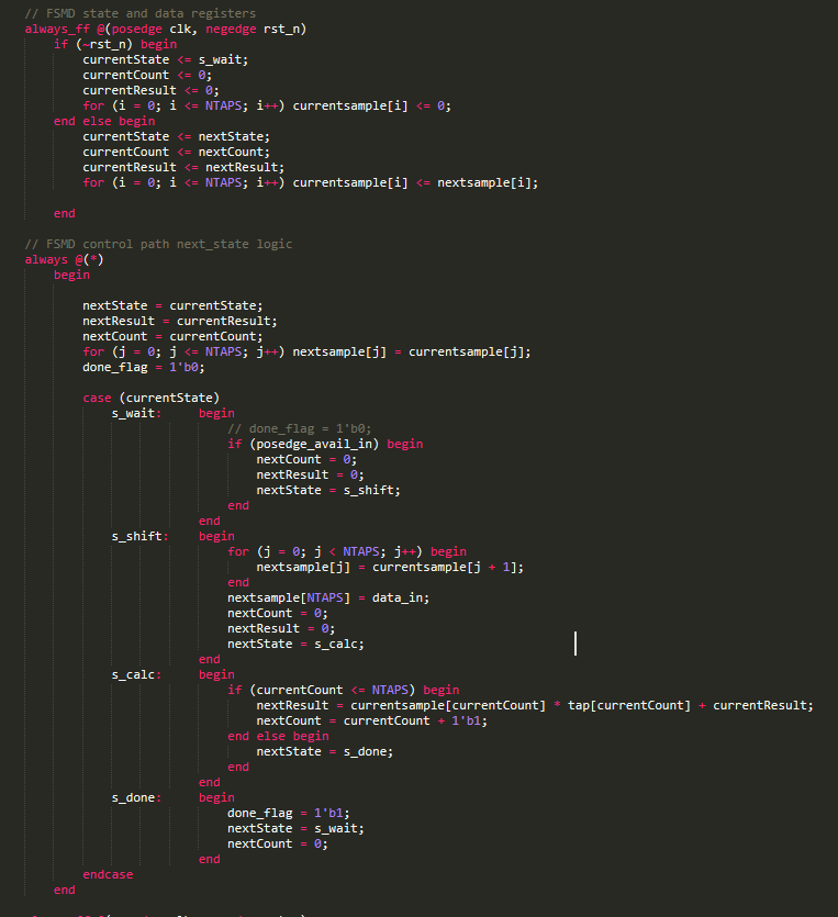
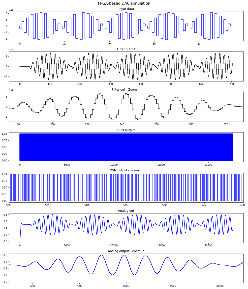
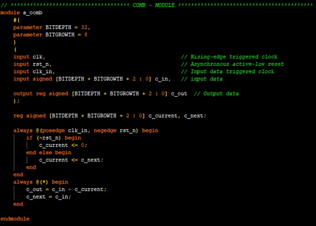
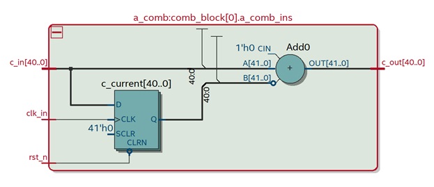
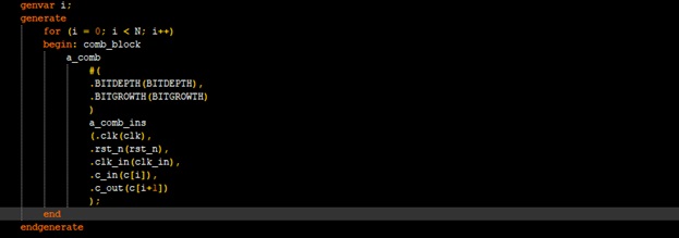
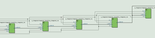
Implementing a FIR filter on FPGA for slow signal

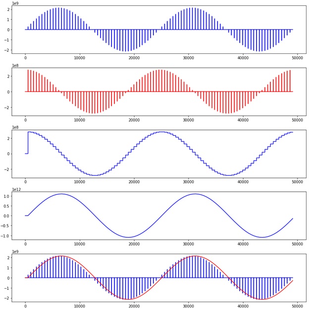
FIR filter for slow signal will designed by using special way to save the number of multipliers.

  1. Finding coefficients using window method
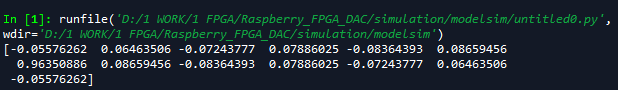
Using Python

from future import print_function
from future import division
import numpy as np

fS = 48000 # Sampling rate.
fL = 22000 # Cutoff frequency.
N = 13 # Filter length, must be odd.

h = np.sinc(2 * fL / fS * (np.arange(N) – (N – 1) / 2))

h /= np.sum(h)
print(h)

Fir characteristics
Coefficients

2. Implementing on FPGA

(Block diagram)
(State machine)
(Finite-state machine with datapath of slow FIR filter)
(Simulation result – using Python + QuestaSim)

Implementing a CIC filter on FPGA

Cascaded integrator–comb filter

Overview

In digital signal processing, a cascaded integrator–comb (CIC) is an optimized class of finite impulse response (FIR) filter combined with an interpolator or decimator.

A CIC filter consists of one or more integrator and comb filter pairs. In the case of a decimating CIC, the input signal is fed through one or more cascaded integrators, then a down-sampler, followed by one or more comb sections (equal in number to the number of integrators). An interpolating CIC is simply the reverse of this architecture, with the down-sampler replaced with a zero-stuffer (up-sampler).

The system function for the composite CIC filter referenced to the high sampling rate, fs is:

Where:

R = decimation or interpolation ratio

M = number of samples per stage (usually 1 but sometimes 2)

N = number of stages in filter

(Cascaded Integrator – comb filter block diagram)

Designing a CIC filter

A Simple Python example code

Implementing a CIC filter on FPGA

Beware of bit growth of CIC filter.

BITGROWTH = N.log2(RM)

  • Implementing Comb stages on FPGA

Verilog code as below is a comb stage, just for your reference


(RTL view of a comb stage)

For designing Comb block with many stage, We can use generate block


(RTL view of Comb bock)
  • Implementing an Integrator stage on FPGA
(RTL view of a integrator stage)

For designing Integrator block with many stage, We can use generate block

(RTL view of Integrator bock)

Using Python to generate test input, then feed to the ModelSim/Questa to simulate Verilog code, then Python read the output.

Simulation result as below

(Full test diagram)