Input : I2S, bitdepth from 16 to 32 bits, sampling rate upto 768khz,
Asynchronous FIFO built-in,
FPGA-based delta-sigma digital to analog converter (DAC),
256-step digital volume,
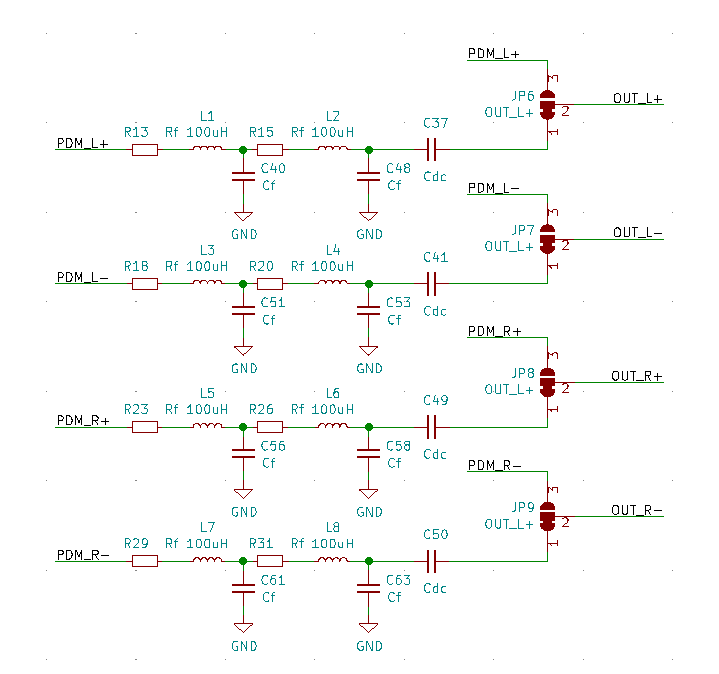
Full balanced outputs,
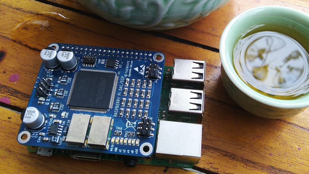
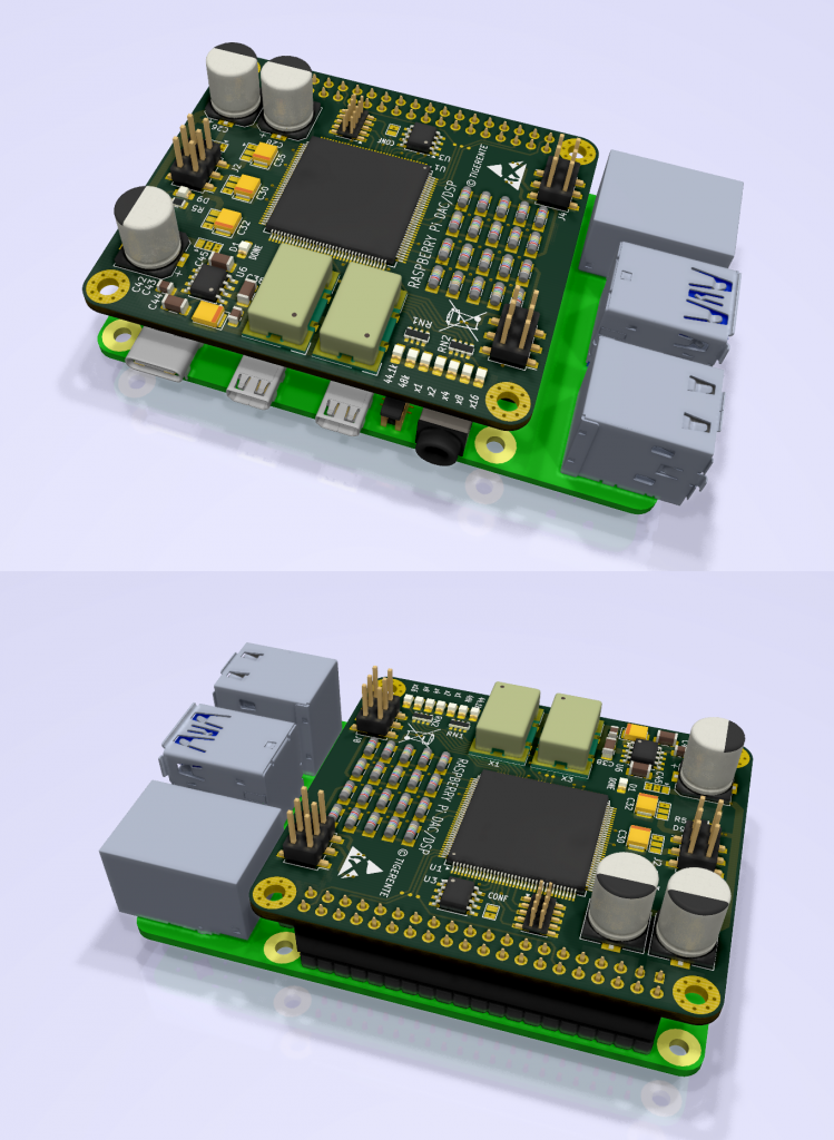
Compatible with Raspberry Pi 3/3B+/4 connection,
Ultra-low phase noise oscillators with high precision linear low drop voltage regulators are designed specifically for High-Definition audio (HD audio).
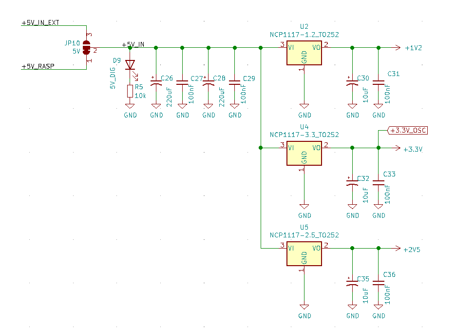
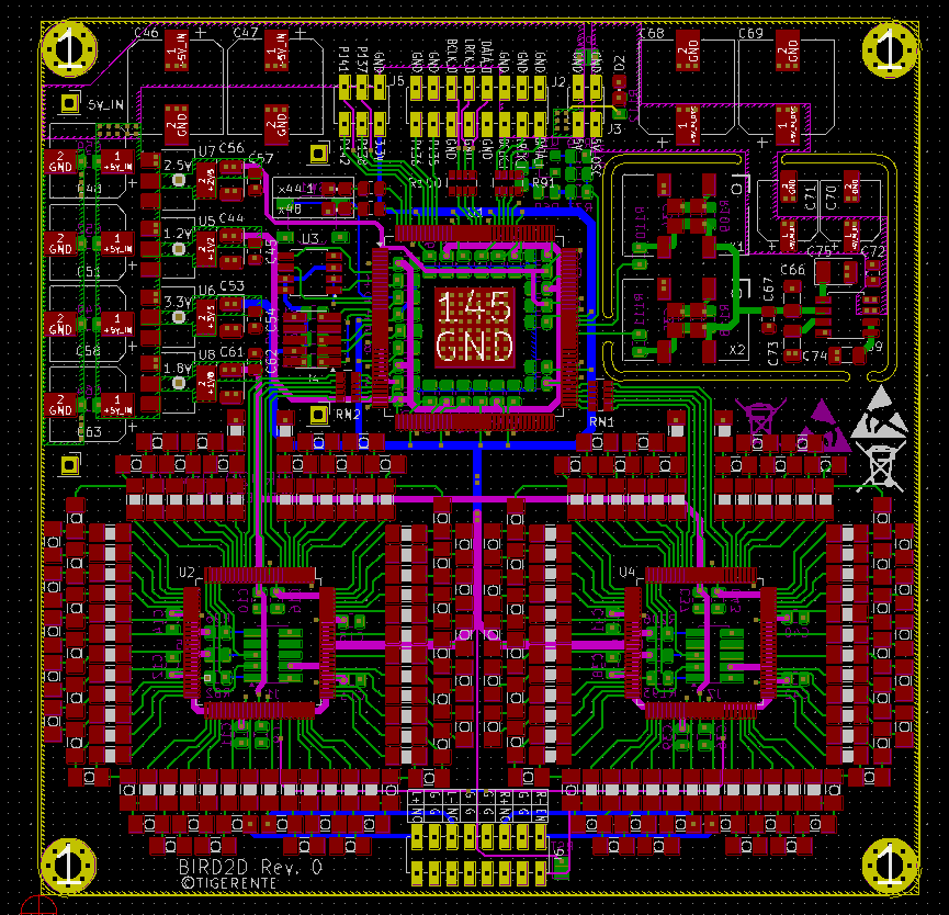
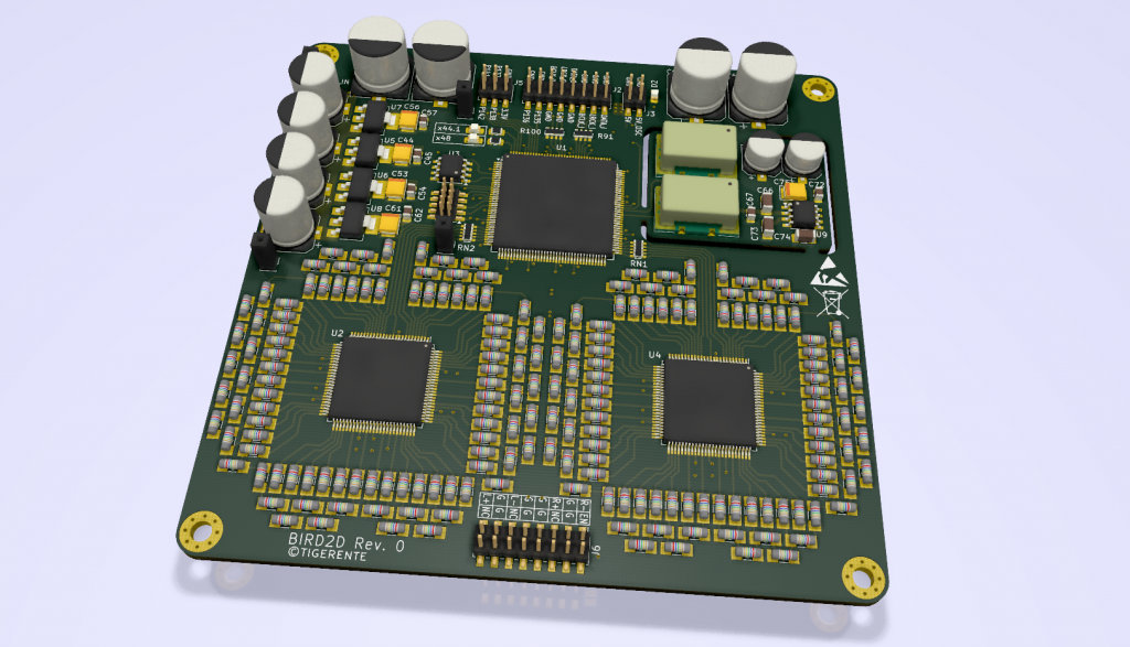
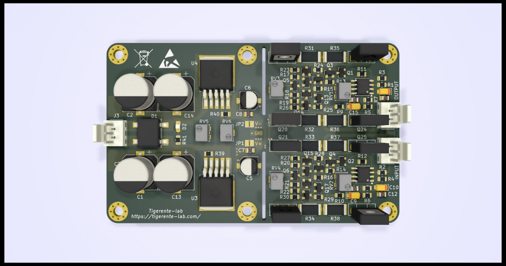
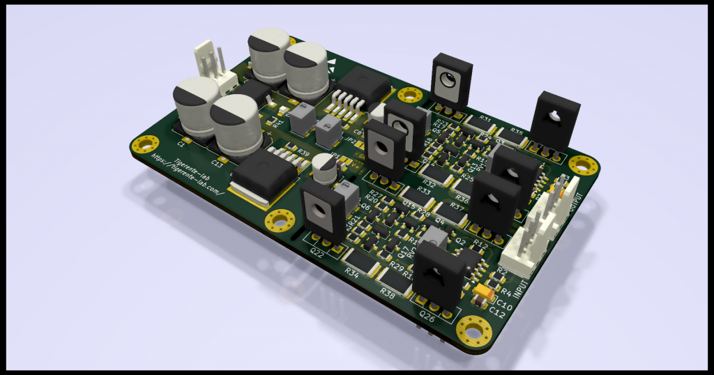
Schematic and PCB design
Schematic and PCB were designed using Free open software KiCad
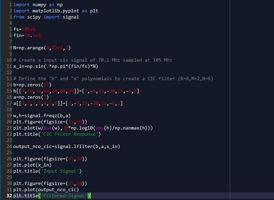
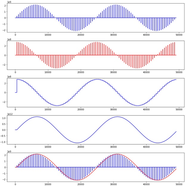
In digital signal processing, a cascaded integrator–comb
(CIC) is an optimized class of finite impulse response (FIR) filter combined
with an interpolator or decimator.
A CIC filter consists of one or more integrator and comb
filter pairs. In the case of a decimating CIC, the input signal is fed through
one or more cascaded integrators, then a down-sampler, followed by one or more
comb sections (equal in number to the number of integrators). An interpolating
CIC is simply the reverse of this architecture, with the down-sampler replaced
with a zero-stuffer (up-sampler).
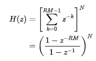
The system function for the composite CIC filter referenced
to the high sampling rate, fs is:
Where:
R = decimation or interpolation ratio
M = number of samples per stage (usually 1 but sometimes 2)
N = number of stages in filter
(Cascaded Integrator – comb filter block diagram)
Designing a CIC
filter
A Simple Python example code
Implementing a CIC
filter on FPGA
Beware of bit growth of CIC filter.
BITGROWTH = N.log2(RM)
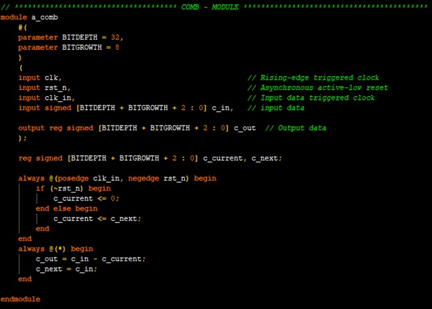
Implementing Comb stages on FPGA
Verilog code as below is a comb stage, just
for your reference
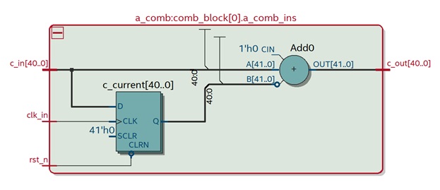
(RTL view of a comb stage)
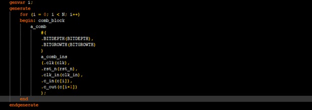
For designing Comb block with many stage,
We can use generate block
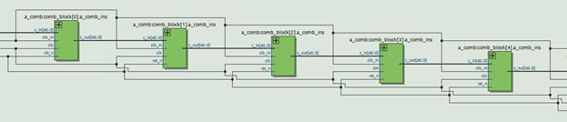
(RTL view of Comb bock)
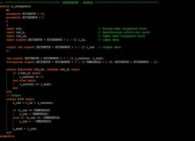
Implementing an Integrator stage on FPGA
(RTL view of a integrator stage)
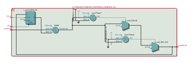
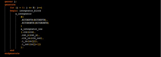
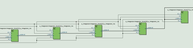
For designing Integrator block with many
stage, We can use generate block
(RTL view of Integrator bock)
Using Python to generate test input, then feed to the
ModelSim/Questa to simulate Verilog code, then Python read the output.
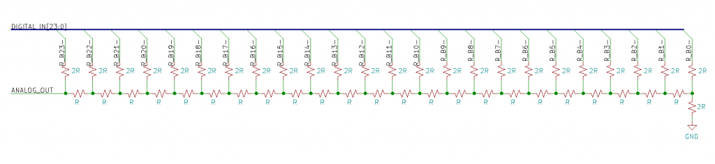
The R-2R resistor ladder network directly converts a parallel digital symbol/word into an analog voltage
(24 bit R-2R resistor ladder)
The R–2R
network causes these digital bits to be weighted in their contribution to the
output voltage Vout. Depending on which bits are set to 1 and which to 0, the
output voltage (Vout) will have a corresponding stepped value between
0 and Vref minus the value of the minimal step, corresponding to
bit 0. The actual value of Vref (and the voltage of logic 0) will depend on the type of
technology used to generate the digital signals.
For a
digital value VAL, of a R–2R DAC with N bits and 0 V/Vref logic levels, the output voltage Vout is:
Vout = Vref * VAL / 2^N
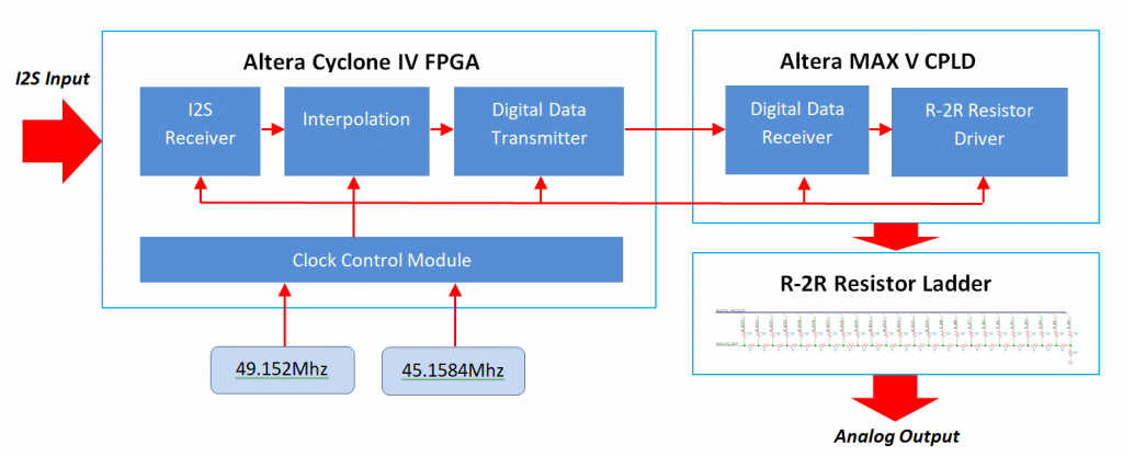
3. Digital Design (Verilog) FPGA-based R-2R resistor ladder DAC
(R-2R
DAC block diagram)
(R-2R DAC RTL
diagram – Quartus Software)
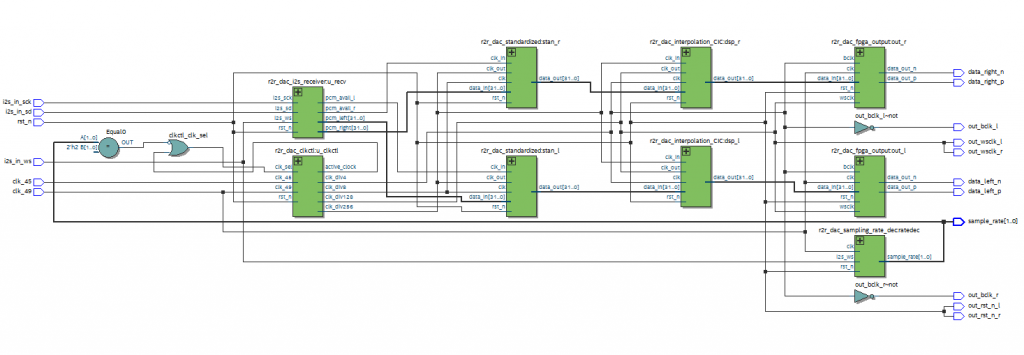
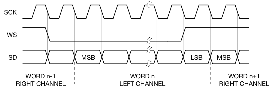
I2S Receiver module:
The I2S
protocol is a common standard used to send audio data. It is a serial protocol
very similar to SPI, but it is a streaming protocol. That means it is always
transmitting data. I2S sends a stream of stereo audio data. For each audio
sample there is a left channel and a right channel value. The values can be any
number of bits, although 16, 20, 24, and 32 bit values are the most common
(I2S
Protocol timing diagram)
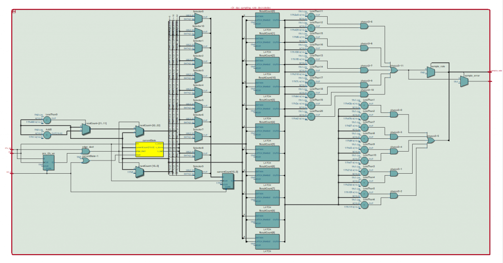
Clock Control Module:
This module includes sampling
rate detect and PLL module.
Sampling rate detect operates
base on the period of Word Clock of I2S (WS) to determines the sampling rate of
I2S. It will be 44.1khz, 88.2khz, 176.4khz, 352.8khz… or 48khz, 96khz, 192khz,
384khz, 768khz. Then this module will choose suitable input OSC (49.152Mhz or
45.1584Mhz) to feed to PLL module.
PLL module uses external clock
that is choose to generate few internal clocks. These clocks are used for
oversampling clocks, filter clocks, R-2R transmitter clocks
(PLL module RTL diagram – Quartus Software)
Interpolation filter module:
Digital data transmitter:
Digital data transmitter module
receives data from Interpolation filter module, converts digital data from
single-end to balanced data and transmits R2R driver module (Altera Max V CPLD)
Data transmit protocol is my
protocol, it is not standard protocol. It is a bit stream protocol and Left /
Right are transmitted separately.
(Digital data transmitter RTL diagram – Quartus Software)
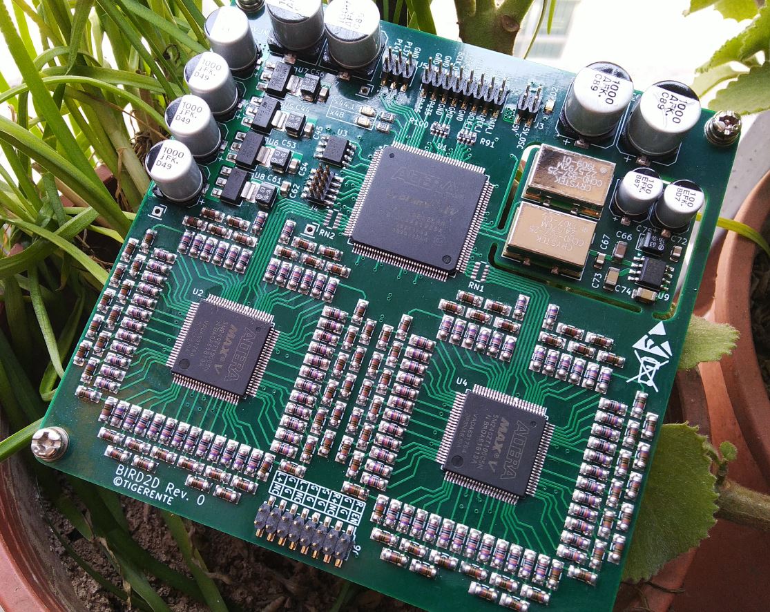
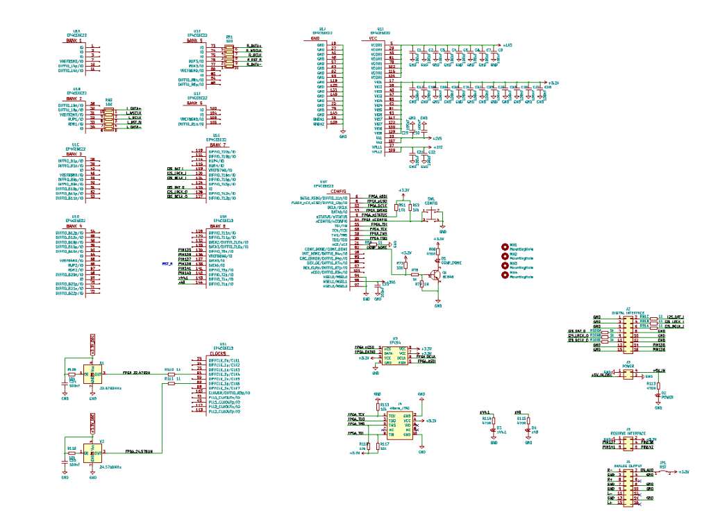
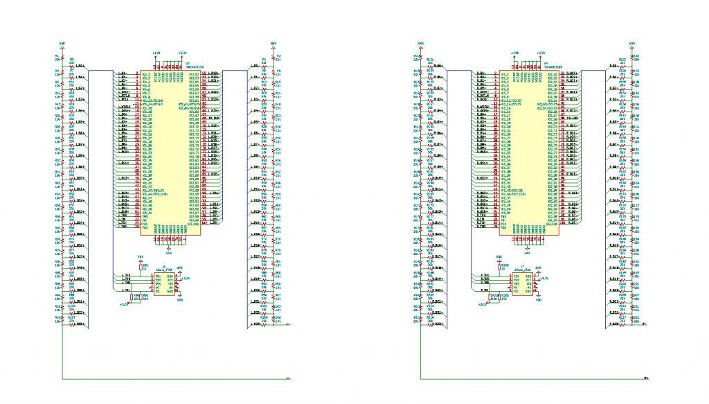
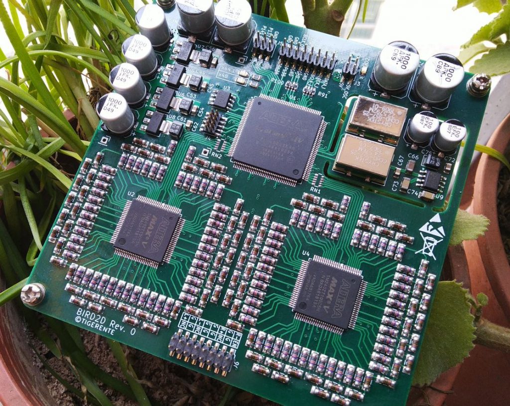
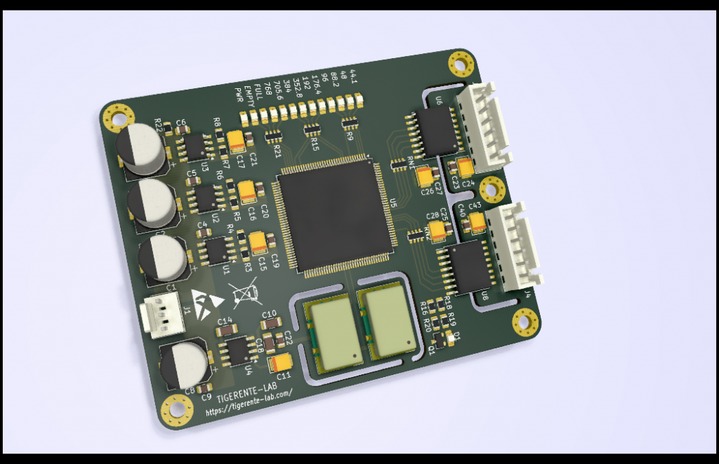
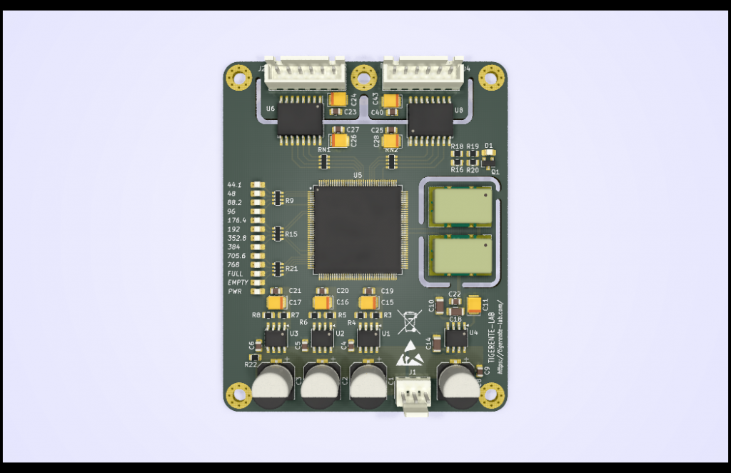
4. PCB Design FPGA-based R-2R resistor ladder DAC
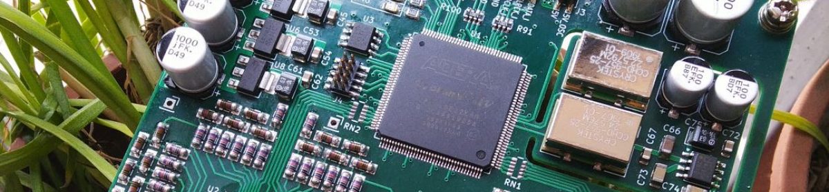
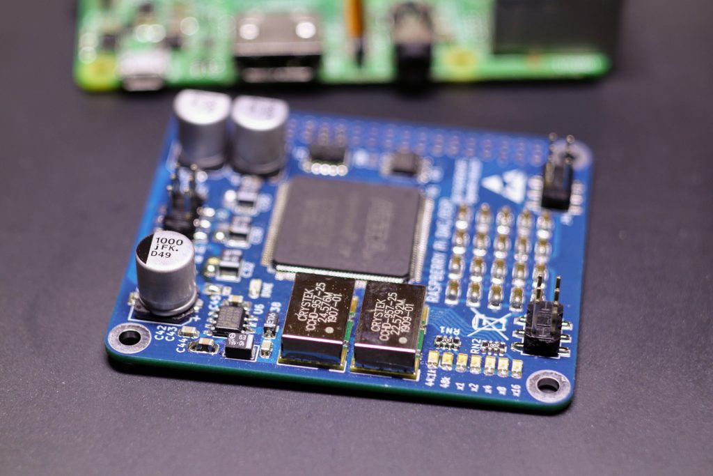
PCB includes 2 parts : FPGA using Altera Cyclone IV and CPLD using Altera MAX V
FPGA Part
FPGA Part uses Altera Cyclone IV EP4CE6 –
144TQFP package
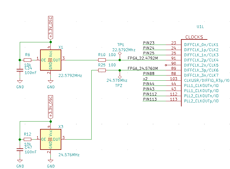
Oscillators use CRYSTEK CCHD-957. Crystek’s
Model CCHD-957 HCMOS CLOCK oscillator family has been designed specifically for
High Definition Audio (HD Audio). It features a typical low close-in phase
noise of -100 dBc/Hz @ 10 Hz offset, and a noise floor of -169 dBc/Hz. With
this extreme low phase noise performance, you will “Hear the Difference”.