Cascaded integrator–comb filter
Overview
In digital signal processing, a cascaded integrator–comb (CIC) is an optimized class of finite impulse response (FIR) filter combined with an interpolator or decimator.
A CIC filter consists of one or more integrator and comb filter pairs. In the case of a decimating CIC, the input signal is fed through one or more cascaded integrators, then a down-sampler, followed by one or more comb sections (equal in number to the number of integrators). An interpolating CIC is simply the reverse of this architecture, with the down-sampler replaced with a zero-stuffer (up-sampler).
The system function for the composite CIC filter referenced to the high sampling rate, fs is:
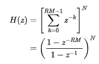
Where:
R = decimation or interpolation ratio
M = number of samples per stage (usually 1 but sometimes 2)
N = number of stages in filter
(Cascaded Integrator – comb filter block diagram)
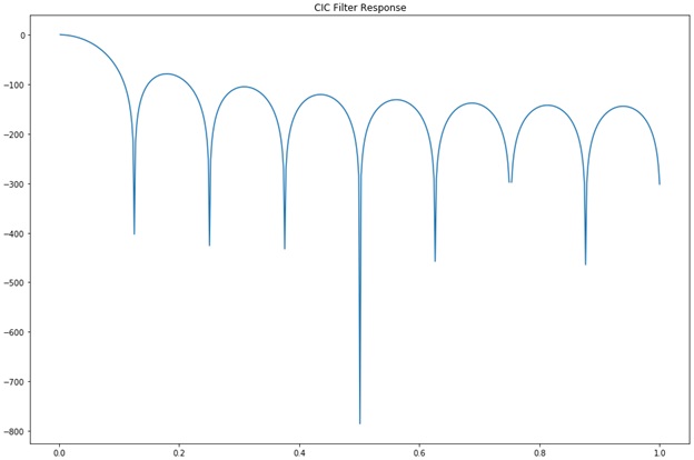
Designing a CIC filter
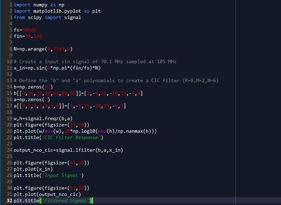
A Simple Python example code
Implementing a CIC filter on FPGA
Beware of bit growth of CIC filter.
BITGROWTH = N.log2(RM)
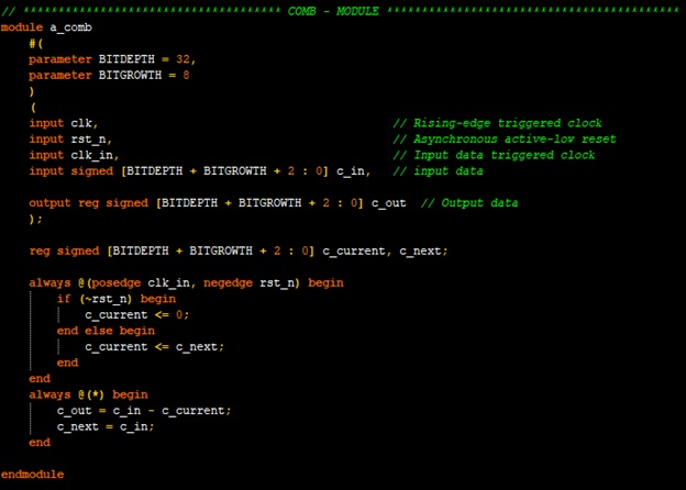
- Implementing Comb stages on FPGA
Verilog code as below is a comb stage, just for your reference
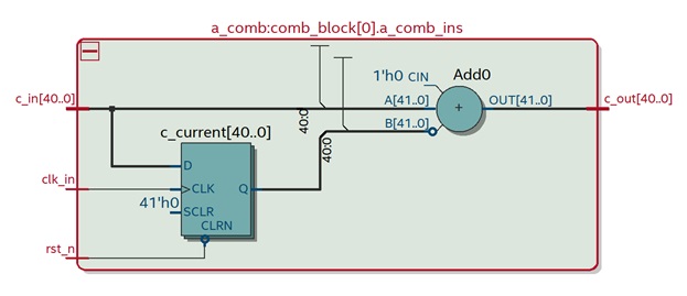
(RTL view of a comb stage)
For designing Comb block with many stage, We can use generate block

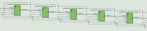
(RTL view of Comb bock)
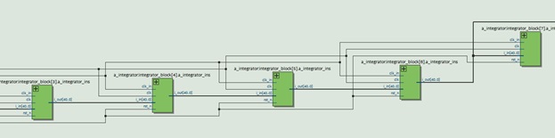
- Implementing an Integrator stage on FPGA
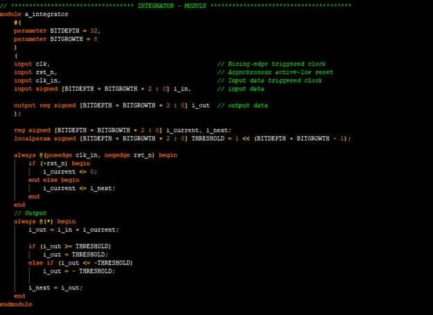
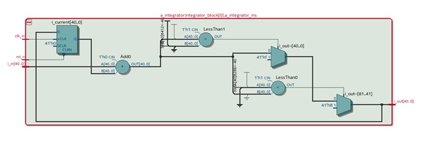
For designing Integrator block with many stage, We can use generate block

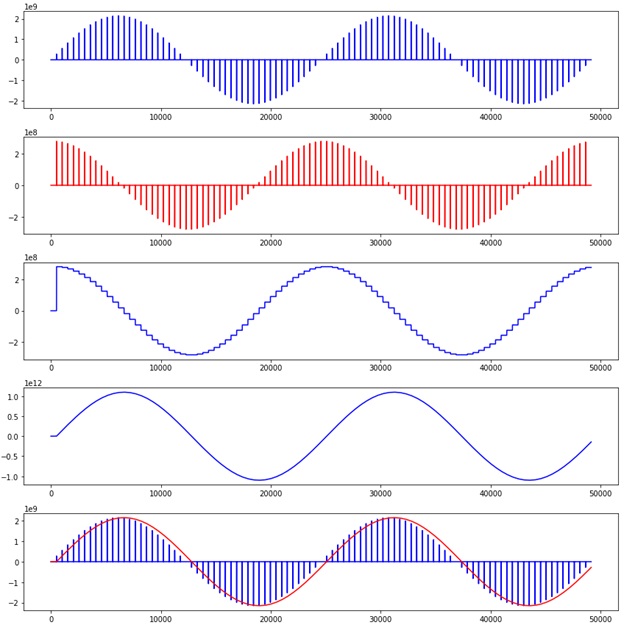
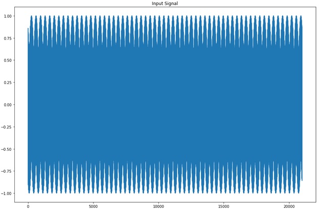
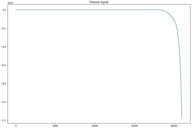
Using Python to generate test input, then feed to the ModelSim/Questa to simulate Verilog code, then Python read the output.
Simulation result as below